Build instructions
Before you begin
Please know the current status of the project.
Currently we are working hard to make new developments for the Plastic Scanner.
The first item we are releasing is a development board, this needs to be taken quite literally, it is for developing purpose. With this board you can help develop the Plastic Scanner further and do tests to see if it fits your usecase.
Tools required
In order to replicate the development board you need the following tools:
- Flush cutters
- Forceps
- Screwdriver
- Solder
- Patients
- Copper wick
- Good eyes or a cheap usb microscope.
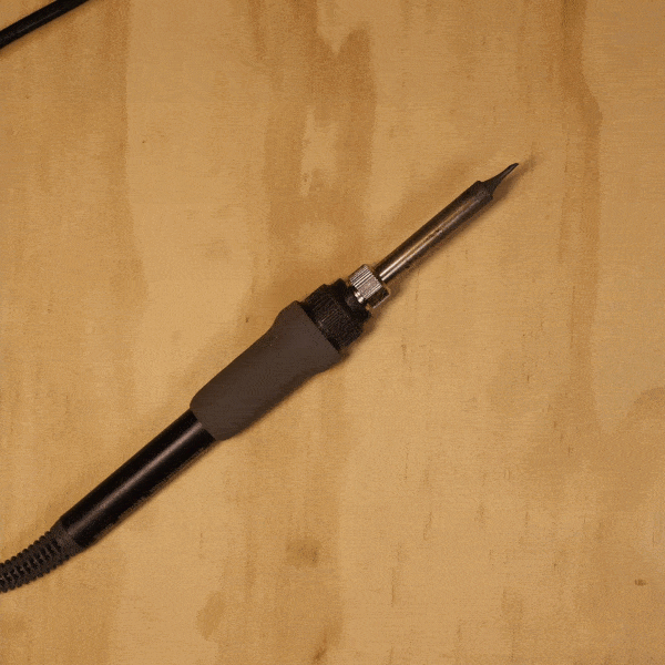
- Themperature controlled soldering iron
- 3D printer
- flux (optional)
Material required
In order to replicate the development board you need the following materials:
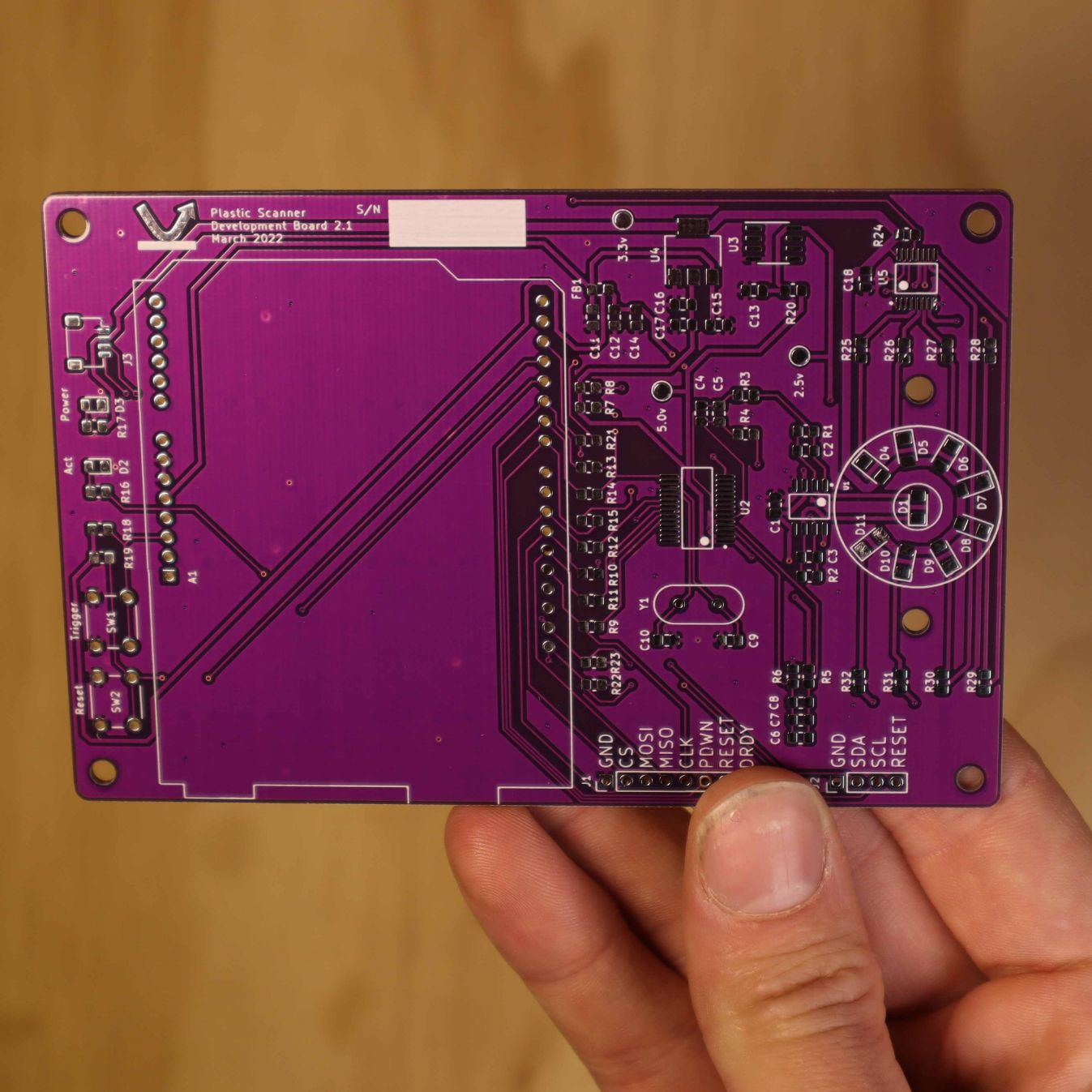
- The printed circuit board
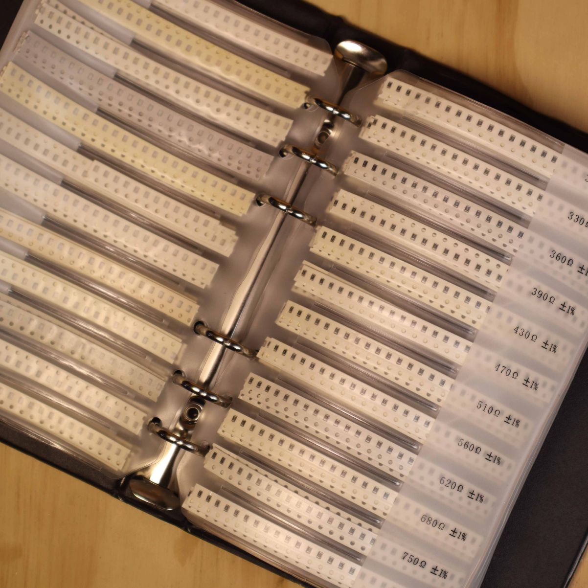
- Bulk components (resistors, capacitors)
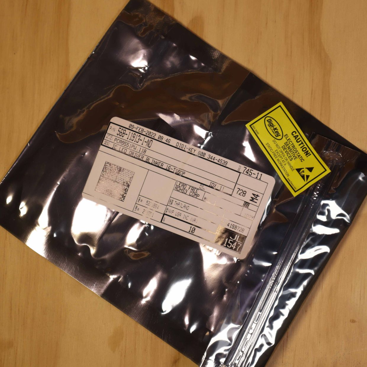
- Specialized components (adc, arduino, IR LEDs)
All the details can be found in the (Interactive) BOM
Electrical Assembly
This pages walks you through all the soldering and testing of the PCB. All components can be soldered with a reflow oven or hot air station, but with some patience you can also solder it by hand. The board consist of 0805 SMD components which are rather easy to solder by hand. the chips can be a bit more difficult to solder but with some solder and solderwick you will manage.
The board will be soldered in 4 area's after soldering each area you can test to see if the board gives the desired results.
Area 1 - Power
We start by soldering the power components, once this area is complete we can measure the voltages to check if they are correct.
-
Solder C1, C2, C3, C4, C5, C6 in place
-
Solder L1, U1, U2, Led1,Led2, R1,R2,R3 in place
-
Supply 5 volts and ground to pin 3 and pin 2 of the external device connector. The LED's in the lower right corner should now light up.
You can measure if they have the correct voltages by measuring on the right side of the LED and the left side of the corrisponding resistor (R2, R3, R4).
The voltage between the left side of R2 and the right side of LED1 should be 5.0 volts.
The voltage between the left side of R3 and the right side of LED2 should be 3.3 volts.
The voltage between the left side of R4 and the right side of LED3 should be 2.5 volts.
If all is correct you can proceed to the second area!
Area 2 - ADC
We continue by soldering the ADC related components in place.
- Solder the ADC in place (how)
- Make sure all connections are properly soldered and there are no bridges.
- Solder R9,R10,R13,R14,R15,R16,R17,R18,R19,R20,R21,R22,R23 (but not R24)
- Solder C12,C14,C16,C17,C18 and X1
- Solder the pinheaders for the arduino in place
- Solder the LogicAnalyzer connector with the notch on the left side.
- Place the Arduino Uno upside down on the headers with the USB port facing the left side
Once you have reaced this stage you are very well on your way! It is now time to see if all connections are good and if the Arduino Uno can communicate to the ACD. Upload the selftest.ino file onto the arduino and open the serial monitor for see the responce.
Area 3 - Analog front
The next step is being able to measure infrared light. The analog front convert infrared light into a voltage source so that it is possible to measure small changes.
- Solder the U3 in place
- Make sure all connections are soldered and there are no bridges
- solder R5,R6,R11,R12 in place
- Solcer C7,C8,C9,C13,C15 in place
- Solder a 0 ohm resistor at C10 and C11
- Solder the InGaAs photodiode in place
If all is correct you now have a very sensitive infrared brightness meter. To check if it is working you can use a TV remote and see the responsitivity on the serial plotter!
Area 4 - LEDs
The last step in the process is the most expensive part, we want to make sure the PCB is good before we continue with this section.
- Solder U4 in place
- Make sure all connections are soldered and there are no bridges
- Solder R26,R27,R28,R29,R30,R31,R32,R33 in place
- Solder D1 to D8 in place, these are the specific wavelength LEDs, start with the lowest value at D1 (850nm) all the way to the highest value at D8 (1650nm), Make sure to LED is nice and flat on the PCB and only solder for 3 seconds before cooling down the PCB again.
That is it! You just soldered the whole development board by yourself! Great job!